
Abstract
Lithium niobate (LiNbO3) is a crystalline material which is widely applied in surface acoustic wave, microelectromechanical systems (MEMS), and optical devices, owing to its superior physical, optical, and electronic properties. Due to its low toughness and chemical inactivity, LiNbO3 is considered to be a hard-to-machine material and has been traditionally left as as an inert substrate upon which other micro structures are deposited. However, in order to make use of its superior material properties and increase efficiency, the fabrication of microstructures directly on LiNbO3 is in high demand. This paper presents an experimental investigation on the micro machinability of LiNbO3 via micro milling with the aim of obtaining optimal process parameters. Machining of micro slots was performed on Z-cut LiNbO3 wafers using single crystal diamond tools. Surface and edge quality, cutting forces, and the crystallographic effect were examined and characterized. Ductile mode machining of LiNbO3 was found to be feasible at a low feed rate and small depth of cut. A strong crystallographic effect on the machined surface quality was also observed. Finally, some LiNbO3 micro components applicable to sensing applications were fabricated.
Export citation and abstract BibTeX RIS

Original content from this work may be used under the terms of the Creative Commons Attribution 3.0 licence. Any further distribution of this work must maintain attribution to the author(s) and the title of the work, journal citation and DOI.
1. Introduction
Single crystal lithium niobate (LiNbO3) has attracted attention from many researchers for its wide range of applications in surface acoustic wave, radio-frequency telecommunications, and optical devices owing to its superior physical, optical, and electronic properties (Wong 2002). In recent years, LiNbO3 has shown potential in microelectromechanical systems (MEMS) and biosensor applications (Okayama 2003) due to the fact that it is superior to silicon-based materials in terms of mechanical and electrical performance. There is an increasing need to fabricate microstructures, such as microfluidic channels and diaphragms, on LiNbO3 directly. However, due to its low toughness, high anisotropy, and chemical inactivity, LiNbO3 is considered to be a hard-to-machine material and has been traditionally left as an inert substrate upon which other micro structures are deposited (Tseng 2006, Johansson, 2012, Sridhar 2012).
Interestingly, although mechanical grinding has been used to dice LiNbO3, very little research has been reported on employing mechanical micro cutting approaches in shaping LiNbO3 micro structures. Micro milling, an emerging micro manufacturing process, has been successfully applied to the fabrication of 3D complex-shaped micro components with excellent dimensional accuracy and surface finish over a variety of engineering materials (Cheng 2013). Recently it has been successfully applied in machining brittle materials and crystals, such as graphite (Huo 2014), single crystal silicon (Rusnaldy 2007, 2008, Arif 2012, Choong 2015, Huo 2015), ceramics (Cho 2007) and glass (Foy 2009, Arif 2011). Micro milling is therefore expected to have the potential to cost effectively fabricate complex-shaped LiNbO3 micro components with feature sizes at the order of several tens to several hundred microns. Success of micro milling LiNbO3 will open new industrial avenues in the fabrication of LiNbO3 micro products and fill the gap of fabrication of micro/meso scale components for prototype or small batch production.
In this paper, an experimental investigation is presented on the micro machinability of LiNbO3 via micro milling with the aim to obtain optimal process parameters. Machining of micro slots was performed on single crystal LiNbO3 wafers using single crystal diamond tools. Surface and edge quality, cutting forces, and crystallographic effects were examined and characterized. Based on results obtained from the machinability study, some LiNbO3 micro components applicable to sensing applications were fabricated.
2. Current fabrication techniques
Device shaping on LiNbO3 has been continuously reported for being difficult to machine. This is because LiNbO3 is highly anisotropic, brittle, inert to most etchants and transparent to most laser wavelengths (Lee 1995). Manufacturing processes, namely wet or dry etching, laser micromachining and mechanical micromachining methods had been researched for fabricating profiles such as micro-channels on LiNbO3. With the increasing need for a precise etching technique, research to enhance the chemical reactivity for wet etching was focused through the development of ion implantation approaches. These processes include focused ion beam (FIB) milling, reactive ion beam etching and deep reactive ion etching (DRIE) (Wong 2002).
Sridhar et al performed FIB milling to fabricate micro-channels in LiNbO3 (Sridhar et al 2012). Y- and Z-cut samples were used and micro-channels 10 μm long with widths of 1 and 0.5 μm were fabricated at three different ion currents. Results showed that the material removal rate decreases with respect to the aspect ratio of the final milled structure when the ion dose increases. Low aspect ratio structures can therefore be milled directly, however material re-deposition is needed if deeper structures with a high aspect ratio are required. With the involvement of argon, reactive ion beam etching allows a higher material removal rate when compared to FIB milling (Chapman 1984). DRIE was also studied and shown to achieve better etching results compared to FIB milling and reactive ion beam etching (Darbyshire 1986). Using lower pressure plasma and placing the sample in a DC bias, the sample is attacked by both chemical reactions with plasma ions and also directional ions which bombard the substrate when accelerated across the cathode (Winnall 2000). This allows the etching rate to increase due to the generation of higher ion energies.
Laser micromachining was also researched for direct fabrication on LiNbO3. Greuters et al performed laser micromachining using 355 nm Nd:YVO4 and 193 and 248 nm excimer lasers (Greuters and Rizvi 2003). Good quality results were obtained from the 355 nm and both excimer lasers. In addition, the crystallographic orientation effect was deemed to be insensitive when compared to those of DRIE (Winnall and Winderbaum 2000). Malshe et al performed laser micromachining using a femtosecond laser. A distinct advantage of a femtosecond laser compared to those of micro or nanoseconds is the redeposition due to ultrashort lasing pulses (Malshe et al 2004). A thin layer of amorphous region was identified on the surface after laser micromachining. Lin et al also performed laser micromachining with a femtosecond laser to create a free standing microresonator (Lin et al 2015). The entire machining process involved femtosecond laser micromachining with FIB milling and high quality microresonators were produced.
Although wet etching, ion implantation, FIB milling and laser micromachining have been studied for device shaping of LiNbO3, these processes suffer relatively low material removal rate and are only economical for high volume production. Alternatively, mechanical micromachining also shows potential in LiNbO3 manufacturing. Okuda et al conducted planer-type cutting using diamond tools to fabricate micro grooves with varying depth up to 50 μm and confirmed that the edge quality of the groove affects the propagation mode of the surface acoustic wave (Okuda 2014). Takigawa et al employed ultra-precision cutting in the fabrication of LiNbO3 ridged waveguides (Takigawa 2014). A smooth finish of approximately 4.5 nm was achieved on the machined sidewalls and thus reduces scattering losses of guided light. Currently, investigations on micro milling of LiNbO3 are very limited, notably, Al-Shibaany et al performed hole drilling experiments using end milling and characterised the sub-surface strains using Raman spectroscopy (Al-Shibaany et al 2014); Shizuka et al (2010) conducted micro milling experiments using tungsten carbide tools and discussed the crystallographic effect. The feasibility of forming micro grooves was proven and the ductile mode was observed to be at a 5 μm depth of cut or less (Shizuka et al 2010).
3. Experiments
3.1. Experimental setup
Experiments for this work were carried out on an ultra-precision desktop micro machining centre (Nanowave MTS5R). The machine is equipped with a high speed aerostatic bearing spindle (Air Bearings Ltd) offering a speed of 18 000 rpm–180 000 rpm. The high speed spindle allows a high cutting velocity even when small diameter cutters are used. The XYZ sliders provide a precision of 0.1 μm. This experimental set-up ensures that both the spindle errors such as vibration and run-out, and slideway inaccuracy were minimised. Therefore spindle and slideway errors on surface quality will not be explicitly taken into account in the analysis. A multi-component piezoelectric cutting force dynamometer (Kistler MiniDyn type 9256C2) was mounted on the top of a Z slide to monitor the cutting force during machining and also assist the cutting tool set-up. The experimental set-up is illustrated in figure 1.
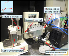
Figure 1. Experimental set-up and working coordinates.
Download figure:
Standard image High-resolution imagePolished Z-cut LiNbO3 samples (dimension 10 mm × 10 mm × 0.5 mm) were used in this research. The samples were adhesively bonded onto a ground stainless steel fixture and removed using acetone after machining. Single flute single crystal diamond micro milling tools (Contour Fine Tooling) with a nominal diameter of 0.3 mm were used in the experiments. A uniform tool shank diameter of 3 mm is used for all micro tools to fit a 3 mm ultra-precision spindle collet. Figure 2 shows the micro end mills used in the experiments.
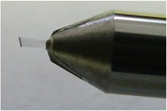
Figure 2. Single crystal diamond micro milling tool used in the experiments.
Download figure:
Standard image High-resolution image3.2. Experimental procedure
Prior to the machining experiments, the levelness of the square LiNbO3 wafer surface to the cutting tool axis was carefully adjusted using a 1 μm resolution dial gauge. A levelness deviation of less than 5 μm was obtained over the 10 mm × 10 mm machining area. To eliminate the effect of levelness deviation on the depth of cut, the NC program (Z feed) was also adjusted to compensate for this geometric error thanks to the 0.1 μm feed precision of the machine tool. Zero position of the cutting tool relative to the LiNbO3 wafer surface was set with the assistance of a machine vision system (Dino-lite microscope) and initial contact test using the Kistler dynamometer at a very slow feed rate. This procedure allows one to set up the depth of cut at a micron level.
Full immersion slot milling was performed in this experiment. No coolant was used to avoid contamination, and compressed air was supplied throughout the machining experiments to reduce the possibility of chip jam induced micro cracks. Two sets of machining experiments were carried out to investigate the influence of the cutting parameters and crystallographic effect on the surface quality, respectively.
In the first set of experiments, 5 mm long and 0.3 mm wide micro slots were milled along a fixed ![$\left[1\,0\,\bar{1}\,0\right]$](https://content.cld.iop.org/journals/0960-1317/26/9/095005/revision1/jmmaa25f4ieqn001.gif) direction. The three controlled quantitative factors used in the experiments are cutting speed (m min−1), feed rate (μm/tooth) and axial depth of cut (μm). Due to the presence of only three controlled factors, full factorial experimental designs were implemented to capture the entire main effects and their interactions. Two levels of cutting speed, three levels of depth of cut, and four levels of feed rate were selected. The cutting parameters in this 2 × 3 × 4 mixed level full factorial design is presented in table 1. Each set of cutting parameters was repeated to reduce machining errors and separate the influence due to interactions from the measurement noise. A total of 48 slots were machined for each cutter. In order to reduce the influence of tool wear on the surface quality and edge chipping, a brand new micro tool was used for the experiments.
direction. The three controlled quantitative factors used in the experiments are cutting speed (m min−1), feed rate (μm/tooth) and axial depth of cut (μm). Due to the presence of only three controlled factors, full factorial experimental designs were implemented to capture the entire main effects and their interactions. Two levels of cutting speed, three levels of depth of cut, and four levels of feed rate were selected. The cutting parameters in this 2 × 3 × 4 mixed level full factorial design is presented in table 1. Each set of cutting parameters was repeated to reduce machining errors and separate the influence due to interactions from the measurement noise. A total of 48 slots were machined for each cutter. In order to reduce the influence of tool wear on the surface quality and edge chipping, a brand new micro tool was used for the experiments.
Table 1. Cutting parameters used in the first set of experiments.
| Cutting parameters | Values |
|---|---|
| Feed per tooth (μm/tooth) | 0.1, 0.3, 0.6, 1.0 |
| Axial depth of cut (μm) | 1, 5, 10 |
| Spindle speed (rpm) | 20 000, 50 000 |
In the second set of experiments, 5 mm long and 0.3 mm wide micro slots were milled along various crystallographic directions for studying the crystallographic orientation effect. The cutting parameters were fixed using optimal cutting speed and feed rate obtained from the first set of experiments. Figure 3 shows the schematic feed direction in the second experiments.
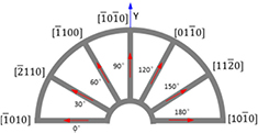
Figure 3. Feed directions in the second set of experiments.
Download figure:
Standard image High-resolution imageAfter the machining experiments, the machined surface was cleaned in acetone by an ultrasonic bath. The average surface roughness of the bottom surface for each micro-milled slots was then measured using a white light interferometer (Zygo NewView 5020). To reduce the measurement uncertainty, four measurements on different areas were conducted for each slot and an average value of surface roughness (Ra) is used for analysis. The surface morphology and burr formation were analysed on the basis of SEM micrographs. Cutting forces and specific cutting energy were calculated and analysed.
4. Results and discussion
Both qualitative and quantitative analyses were carried out to characterise surface and edge quality of micro-milled slots. Qualitative analysis includes burrs formation, cutting mode observation, and surface topography, and quantitative analysis includes surface roughness and specific cutting energy analysis.
4.1. Surface topography and edge chipping
Surface characterisation of the machined slots was performed using an SEM and a 3D surface profilometer. Figure 4 shows the SEM micrographs of the micro machined slots. Surface defects were found on the micro machined surface and edge chipping was observed in most of the slots. The results show that the feed rate and axial depth of cut have significant influence on the surface generation. Higher cutting speed is also found to promote better surface quality. Slow feed rate and small axial depth of cut produce fewer surfaces defects and hence promote ductile mode machining. Figure 5 shows surface measurement results on typical ductile and brittle mode machined surfaces. On the ductile mode machined surface, regular tool marks and less surface defects were observed. Surface roughness measurements indicate that a very smooth surface with surface roughness Ra = 10 nm can be achieved at fz = 0.1 μm/tooth and ap = 1 μm. In contrast, on the brittle mode machined surface, regular tool marks are absent and instead irregular streaks were observed, and surface roughness, Ra = 50–150 nm, was measured.
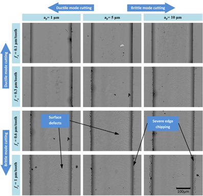
Figure 4. Machined surface topography at different feed rate and depth of cut (cutting speed: 31.4 m min−1).
Download figure:
Standard image High-resolution image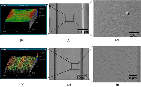
Figure 5. Examples of ductile and brittle mode machined surface: (a)–(c) ductile mode machined surface; (d)–(f) brittle mode machined surface; (a) and (d) Zygo surface profilometer surface roughness measurement.
Download figure:
Standard image High-resolution imageAs already demonstrated in previous single point diamond turning (SPDT) experiments, an enabling factor for ductile mode machining of brittle materials is the use of very small uncut chip thickness and depth of cut. It is believed that there is a critical uncut chip thickness, below which the energy required to cause fracture is higher than that required for plastic deformation. Therefore, plastic deformation becomes the primary mechanism of material removal instead of brittle fracture (Li et al 2010, Yan et al 2009). When materials undergo ductile shear plastic deformation, lesser surface and subsurface defects are generated and hence better surface roughness can be achieved.
Edge chipping is a type of surface/subsurface defect normally induced in the machining of brittle materials. Machining induced edge chipping affects the geometric accuracy of the finished parts and causes potential functional failure due to the micro cracks left on the finished part (Ng 1996, Gong 2013). Good edge quality in some LiNbO3 applications is believed to be more desirable than surface roughness. In the micro milling of micro devices, the size of edge chipping defects can be comparable to its feature size, therefore control and suppression of edge chipping formation in micro milling becomes a pressing challenge. The SEM micrographs in figure 4 show a similar trend as surface topography, i.e. lower feed rate and axial depth of cut would produce less edge chipping defects due to ductile mode machining. In a full immersion milling operation, both up and down milling sides of the slot are generated. In the up milling side, the cutting direction is opposite to the workpiece feed direction and the surface is generated at the beginning of the cut, whilst the cutting direction is the same as the feed direction in the down milling side and the surface is generated when the cutting edge exits the workpiece. Therefore, up and down milling have different characteristics in edge chipping formation. Within the machining conditions in this experiment, edge chipping defects were predominantly observed in the down milling side of the slot, and lesser or no edge chipping in the up milling side were formed as shown in figure 6. Brittle materials like LiNbO3 are more sensitive to impact at workpiece entry. In the case of up milling, the nominal instantaneous uncut chip thickness starts from minimum chip thickness (a few tens of nanometers in this case) and increases gradually, therefore lesser edge chipping defects are formed. This conclusion is in agreement with the micro milling of other brittle materials (Huo 2015).
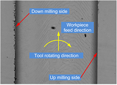
Figure 6. SEM micrographs of micro milled slots showing interior edge chipping.
Download figure:
Standard image High-resolution image4.2. Specific cutting energy
The cutting forces were collected by the dynamometer during the machining process to calculate the specific cutting energy. Firstly, raw force data was used to obtain the principle cutting forces and thrust forces, via equation (1):

where Fx and Fy represent the measured cutting forces along the feed and cross feed directions respectively, while Ft and Fr represent the thrust and cutting forces, and θ is the rotation angle of the cutting. Then specific cutting energy, or specific cutting force (unit: MPa), Uc, is defined as follows:

where Vc and Vrem stand for the cutting speed and material removal volume, with Tc as the cutting time.
It has been proven that the specific cutting energy required by plastic deformation of the material is higher than that required by brittle rupture (Wang 2008). Thus, it would also be an indication of brittle-ductile transition occurring should a drop of the specific cutting force be observed.
Analysis of variance (ANOVA) performed on the cutting force data (figure 7) indicates that, within the experimental machining conditions, a lower depth of cut or a slower feed rate results in higher specific cutting energy, hence indicating that a ductile mode cutting has taken place. As shown in figure 7, when depth of cut of 1 μm is used, a feed rate decrease from a 1 μm/tooth to 0.1 μm/tooth would result in an increase of specific cutting energy from 2000 MPa to 14 000 MPa and also a steep increase from the feed rate of a 0.3 μm/tooth can be observed suggesting that a 0.3 μm/tooth could be the brittle-ductile transition threshold. When a 0.1 μm/tooth is used, a depth of cut decrease from 10 μm to 1 μm would result in an increase of specific cutting energy from 1800 MPa to 14 000 MPa. It can also be seen from figure 7 that a higher cutting speed results in higher specific cutting energy. Therefore, higher specific cutting energy, which has been believed to be a sign of ductile machining, is obtained with higher cutting speed, along with a lower feed rate and cutting depth. This conclusion is consistent with results from the surface topography analysis, which in turn proves that specific cutting energy can be used as an effective indicator of the cutting mode for brittle materials. Attempts were also made to look into the ratio of thrust force and principle cutting force, however, the theory stating that under a critical uncut chip thickness, the thrust force stays larger than the principle cutting force (Davim 2008) was not supported by the results from the micro milling of LiNbO3 in this experiment.
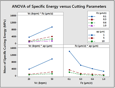
Figure 7. Factorial plots of specific cutting energy versus cutting parameters.
Download figure:
Standard image High-resolution image4.3. Crystallographic effect
In order to study the effect of crystallographic orientation of the material on the surface quality, slots along different crystallographic orientations were machined using single crystal diamond tools using the same cutting parameters, as described in section 3.2. The machining parameters used in the second set of experiments were: spindle speed, n = 50 000 rpm; feedrate, fz = 0.1 μm/tooth; depth of cut, ap = 5 μm. Although almost crack-free surfaces were found to be achieved in the first set of experiments (feedrate, fz = 0.1 μm/tooth and a depth of cut, ap = 1 μm), a slightly deeper depth of cut was used to show the distinct differences along different crystallographic orientations.
Cleavage planes of LiNbO3 naturally run along the family planes of {0 1  2} (Boyd 1964, Weis 1985). Since LiNbO3 has a hexagonal crystalline configuration, it exhibits a three-fold symmetry in which its cleavage planes repeat itself at every 120°. Due to the anisotropy property of the material, a strong crystallographic orientation effect was observed. As shown in figure 8, edge chipping defects were observed in the slots machined along the cleaving directions of
 ![$\left[\bar{2}\,1\,1\,0\right]$](https://content.cld.iop.org/journals/0960-1317/26/9/095005/revision1/jmmaa25f4ieqn003.gif) (30°) and
(30°) and ![$\left[1\,1\,\bar{2}\,0\right]$](https://content.cld.iop.org/journals/0960-1317/26/9/095005/revision1/jmmaa25f4ieqn004.gif) (150°). This is due to the cleaving directions having lower surface energies and hence having less resistance to edge chipping generation during contact with the cutting tool. Good edge quality without obvious chipping defects were achieved by the slots machined other directions. Evident differences on the edge quality were shown between the up-milling and down-milling sides on the machined slots. Surface roughness of the bottom surface along both the feed and cross feed direction were measured. As shown in figure 9, a clear correlation between surface roughness value and crystallographic directions existed. Those slot surfaces machined along 90° have a surface roughness (Ra) of around 40 nm in contrast to those slot surfaces machined along 30° or 150° on which 90 nm Ra was measured. Hence, micro milling should be performed either along or close to
(150°). This is due to the cleaving directions having lower surface energies and hence having less resistance to edge chipping generation during contact with the cutting tool. Good edge quality without obvious chipping defects were achieved by the slots machined other directions. Evident differences on the edge quality were shown between the up-milling and down-milling sides on the machined slots. Surface roughness of the bottom surface along both the feed and cross feed direction were measured. As shown in figure 9, a clear correlation between surface roughness value and crystallographic directions existed. Those slot surfaces machined along 90° have a surface roughness (Ra) of around 40 nm in contrast to those slot surfaces machined along 30° or 150° on which 90 nm Ra was measured. Hence, micro milling should be performed either along or close to ![$\left[\bar{1}\,0\,\bar{1}\,0\right]$](https://content.cld.iop.org/journals/0960-1317/26/9/095005/revision1/jmmaa25f4ieqn005.gif) direction with an up-milling strategy whenever possible for such materials.
direction with an up-milling strategy whenever possible for such materials.
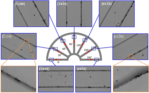
Figure 8. Crystallographic effect on the surface and edge quality.
Download figure:
Standard image High-resolution image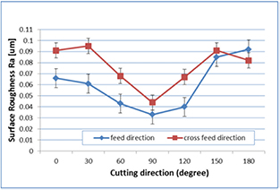
Figure 9. Crystallographic effect on the surface roughness.
Download figure:
Standard image High-resolution image5. Geometry specific fabrication and future work
Resonant based microsensors, which are commonly designed and fabricated from crystalline material to give a high quality factor resonator, offer the opportunity for high resolution measurements at low cost. However initial development costs are high due to the relatively long initial cleanroom preparation time for microfabrication approaches. In order to overcome this issue, the micro milling approach is being developed for prototyping sensors at single or small batch quantities. Piezoelectric single crystal LiNbO3 is a strong material candidate as it allows for a simple sensor design whilst maintaining a high quality factor and good electronic signal recovery. To assess micro milling fabrication performance on specific geometries, polished 0.5 mm thick Z-cut LiNbO3 samples were machined using 0.5 mm diameter single crystal diamond tools. Two test geometries were chosen. A circular diaphragm resonator has applications in mass sensing (Ismail 2006, Ortiz 2012) whilst ridges and channels have applications as waveguides (Hu 2007) and opto-microfluidic sensing (Bettella 2015).
To produce 5 mm diameter diaphragms with 200 μm thickness for prototyping a mass biosensor, circular recesses with 5 mm diameter and depth of 300 μm were fabricated as shown in figure 10(a). Figure 10(b) shows the SEM image of a micro-machined circular diaphragm. Initial results indicate that micro milling produced a smooth vertical sidewall (surface roughness, Ra = 20 nm) and a moderate bottom surface finish (surface roughness, Ra = 80 nm). Figure 11 shows an example of machined LiNbO3 waveguide/microfluidic channels. 300 μm wide by 300 μm deep channels were successfully fabricated. Very smooth vertical wall and good edge quality were obtained, though micro surface defects are still evident on the bottom surface. Performance of these devices is being tested and future work will include investigation of post machining chemical treatments to improve the quality of the machined surface.
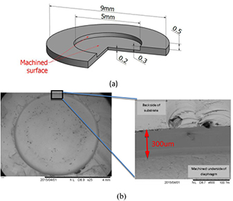
Figure 10. Prototype for biosensors (300 μm depth and 200 μm diaphragm thickness): (a) CAD model; (b) SEM images of machined LiNbO3 diaphragm.
Download figure:
Standard image High-resolution image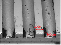
Figure 11. Micro machined channels on a single crystal LiNbO3wafer.
Download figure:
Standard image High-resolution image
6. Conclusions
Micro machining of LiNbO3 crystals was performed by a micro end milling process using single crystal diamond tools. Micro machined surface and edge quality, specific cutting energy, and crystallographic effect were characterised and analysed, with the aim of accomplishing machining in the ductile regime and producing a defect-free surface. The following conclusions can be drawn from this work:
- Surface morphology observation and specific cutting energy analysis revealed that ductile machining on LiNbO3 can be achieved using single crystal diamond end mills at a slow feed rate and low depth of cut, and a threshold of brittle-ductile transition was obtained at a 0.3 μm/tooth under the experimental conditions in this research.
- Specific cutting energy can be used as an effective indicator to predict the ductile model cutting of brittle materials.
- Strong crystallographic orientation effect on the surface and edge quality was observed due to the high anisotropy of the material.
This research has demonstrated that diamond micro milling is a feasible process for the fabrication of LiNbO3 components at a few tens to a few hundred microns scale, and shown how it can be used to translate design to prototypes at a low cost and within a short development time. Future work will be directed towards a post-machining process to remove surface defects and hybrid manufacturing. The results are also expected to be comparable with micro cutting of other brittle materials, such as germanium, silicon, silicon carbide, glass, etc.
Acknowledgments
The authors wish to thank the Engineering and Physical Sciences Research Council (EP/M020657/1, EP/K031953/1) for financial support for this work. The authors are also grateful to Air Bearings Ltd for providing the high speed air bearing spindles which were used in the experiments.