
Abstract
Single-crystalline Al nanowires with diameters under 100 nm are successfully prepared by direct electrodeposition from a room temperature ionic liquid without using templates, additives or catalysts for the first time. We propose the three stages of nanowires growth mechanism including electrodeposition of the initial two dimensional nanofilm, subsequent electrochemical formation of three dimensional nano-nuclei and final one dimensional growth of nanowires. The electrodeposited Al nanowires can grow to lengths of up to 50 μm in 120 s with an average growth rate more than 0.4 μm/s, reaching a high aspect ratio over 1000. This study shows that the dimensions of nanowires are precisely controlled through the variation of electrode potential and are influenced by the electrodeposition temperature and time. The morphology of Al nanowires is very uniform and the nanowire diameters electrodeposited at −1.6 V/25°C within 60 s are in the range of 17 nm to 50 nm. It is found that diffusion strongly influences the growth process.
Export citation and abstract BibTeX RIS
One-dimensional (1D) nanostructures have attracted more and more attention in various fields due to excellent chemical and physical properties. For example, aluminum nanowires have been expected to play important roles as electrode materials for Li-ion batteries1 and Al-air batteries,2 current collectors for 3D micro-batteries,3,4 superconductors in nanoelectronic devices5,6 and potential candidates for field emitters.7 A high-throughput and cost-effective synthesis method is important for practical applications of nanowires.
As a typical bottom-up process, electrodeposition is widely applied to synthesize many sorts of nanostructures since it requires relatively inexpensive equipment and mild reaction conditions.8 One-dimensional nanostructures (nanowires, nanorods and nanotubes) can be electrodeposited with assistant of templates (such as anodic aluminum oxide templates,9,10 track-etched polycarbonate membranes,11–13 lithographical patterns,14 liquid crystalline phases templates15 and step edges on special substrates)16,17 or nanoparticle catalysts (the electrochemical liquid-liquid-solid process).18–20 Nevertheless, cost and time are mainly consumed in preparing and removing the templates or catalysts.
In recent years, it has been discovered that several kinds of metals, such as Sn,21–23 Zn,24,25 Te,26–28 Co,29 Sb,30 Al31–33 and some alloys (Cu-Sn,34 Sn-Si,35 Cu-Zn,36 Ni-Zn,37 Fe-Co-Zn,38 Co-Sm39 and Co-Zn)40 exhibit one-dimensional growth tendency in direct electrodeposition from specific ionic liquids. Some attempts are successful in template-free electrodeposition of wires, rods, belts and tubes under certain conditions accordingly. Several kinds of growth mechanisms such as the overlapping of depletion zones mechanism36 and the selective adsorption of specific species mechanism22 have been proposed. There is a wide variety of ionic liquids because they are composed of organic ions and easily prepared of many components. Nevertheless, the ionic liquids that can be used to directly electrodeposit 1D structures are reported rather limited. According to the recent literatures,31–33 Al sub-microwires with diameter more than 200 nm are prepared by template-free electrodeposition, however the Lewis acidic AlCl3-trimethylamine hydrochloride ionic liquid was the only available electrolyte. Besides, it seems fairly difficult to directly electrodeposit uniform nanowires with diameter under 100 nm in ionic liquids without additional using of templates, catalysts or additives. Moreover, the mechanism of template-free electrochemical 1D-growth in ionic liquids is still incompletely understood.
In this work, we present that uniform single-crystalline Al nanowires with controllable average diameters down to 30 nm can be directly electrodeposited on ordinary metal substrates from the AlCl3/1-butyl-1-methylpyrrolidinium chloride (BMPC) (mole ratio is 2:1) ionic liquid at room temperature. Base on the careful observation and experimental results, we propose an electrochemical 2D nanofilm-3D nanonuclei-1D nanowires (EC 2D-3D-1D) growth mechanism to fundamentally explain the process.
Experimental
All the experiments were performed inside an argon-filled glove box (with O2 and H2O content < 1 ppm). The ionic liquid was prepared by slowly adding AlCl3 (Alfa Aesar, 99.9%) into BMPC (Sigma-Aldrich, 99%) in a beaker and continuously stirred for 24 h. The electrochemical experiments were carried out in a conventional three-electrode cell controlled by a PARSTAT2273 potentiostat/galvanostat with PowerSuite software package. As shown in Figure 2f, a 0.1 mm thick Al plate (Aladdin, 99.99%) was used as the counter electrode (CE). The reference electrode (RE) consisted of a 0.5 mm diameter Al wire (Alfa Aesar, 99.9995%) immersed in the BMPC-AlCl3 ionic liquid contained in a fritted glass tube. A mechanically polished 0.1 mm thick Cu plate (99.9%) was cut into a 5 × 5 mm square with a 0.8 ± 0.2 mm wide "tail" on top (see Figure S1a) and used as the working electrode (WE) for electrodeposition. For the cyclic voltammetric study, a 0.8 mm diameter tungsten wire (99.9%) was used as the working electrode. All the electrodes were cleaned in an ultrasonic cleaner and dried before experiment. To remove the oxide on the surface, the Cu plate was dipped in dilute sulfuric acid for 5 min, washed with deionized water, and dried before experiment. After electrodeposition, the deposits-coated Cu plate was rinsed three times with acetonitrile and dried.
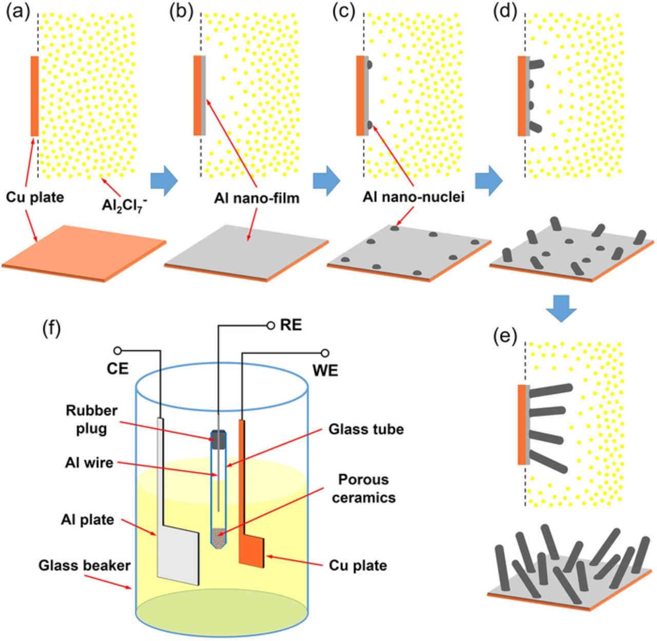
Figure 2. (a-e) Schematic of the EC 2D-3D-1D growth mechanism of the Al nanowires directly electrodeposited on Cu substrate from the AlCl3-BMPC room temperature ionic liquid. (f) Schematic of the three-electrode cell used for the electrochemical experiments.
Viscosity of the ionic liquid was measured using a programmable rheometer (Brookfield LVDV-III ULTRA) with spindles (SC4-31) and sample chamber (SC4-13RP) at a shear rate of 51 s−1 inside an argon-filled glove box (with O2 and H2O content < 1 ppm). The deposits were characterized by scanning electron microscopy (SEM, FEI NOVA Nano SEM450), energy dispersive X-ray spectroscopy (EDS, EDAX TEAMEDS), transmission electron microscopy and high-resolution transmission electron microscopy (TEM/HRTEM, JEOL JEM-2100), selected area electron diffraction (SAED, JEOL JEM-2100) and X-ray diffraction (XRD, Rigaku D/max 2550 VB/PC with Cu Ka1 radiation, the scanning range was from 10° to 80° and the scanning speed was 5° min−1).The TEM sample was prepared as follows. Firstly, the electrodeposited nanowires were ultrasonic dispersed in acetonitrile (99.9%, Adamas) for 20 min. Subsequently, the dispersed nanowires were carefully mounted on 200 mesh lacey-carbon copper TEM grids followed by vacuum drying for 2 h.
Results and Discussion
Ionic liquids exhibit unique properties such as good thermal stability, very high ionic conductivity, large operating potential range, nonvolatility, and nonflammability.8 Bulk aluminum film can be electrodeposited in the Lewis acidic chloroaluminate ionic liquids. Al2Cl7− is considered as the active species and the reaction is carried out according to Equation 1.41
![Equation ([1])](https://content.cld.iop.org/journals/1945-7111/165/13/D641/revision1/d0001.gif)
A typical cyclic voltammogram of AlCl3-BMPC (mole ratio is 2:1) on tungsten wire at 25°C is shown in Figure 1a. The electrode potential was scanned initially from the open circuit potential to the negative direction at a scan rate of 50 mV s−1. The sharp rise in reduction current and the stripping peak upon scan reversal in the cyclic voltammogram indicate that the electrodeposition of Al is reversible and the bulk electrodeposition of Al occurs after −0.1 V (vs. Al/Al3+). The obvious reduction current loop can be attributed to the nucleation and growth of Al on the working electrode.
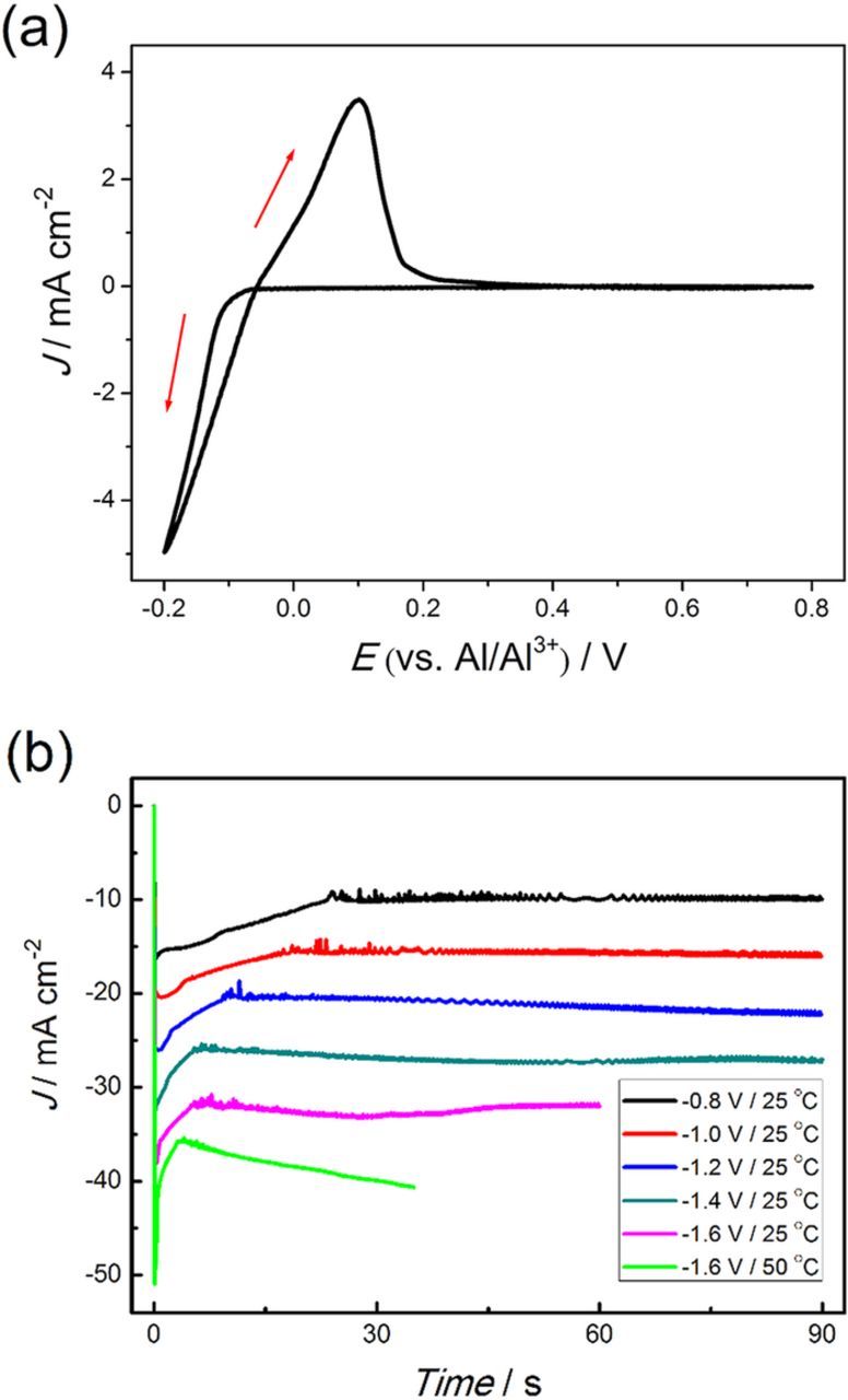
Figure 1. (a) Cyclic voltammogram of AlCl3-BMPC (mole ratio is 2:1) at a scan rate of 50 mV s−1 on W wire at 25°C. (b) The chronoamperometry curves recorded on Cu plate during the electrolysis at various conditions.
In the potentiostatic electrodeposition from the AlCl3-BMPC (mole ratio is 2:1) room temperature ionic liquid, the deposits exhibit apparent 1D growth tendency when the applied potential is more negative than −0.4 V (vs. Al/Al3+). While a potential more negative than −0.8 V (vs. Al/Al3+) is applied, Al nanowires with average diameters less than 100 nm can be directly electrodeposited on Cu substrates at room temperature in our experiments. According to our investigations, the formation of Al nanowires can be divided into three stages: predeposition of a shiny Al nano 2D thin film, 3D nucleation of Al on the thin film and 1D growth of Al nanowires. This EC 2D-3D-1D growth process as shown in Figures 2a–2e also occurs on other substrates (W, Mo, Ni and so on) and at higher temperatures in our experiments.
As presented in Figure S1, the shiny pre-deposited Al nanocrystalline thin film is obtained on Cu substrate in a short time after a negative potential is applied. The top view SEM images (Figure S1d, Figure S1i and Figure 5a) show that the Al nanocrystalline thin films are quite uniform and consist of fine grains within 100nm. To investigate the Al nano thin film without serious damage, the film was partially peeled-off the Cu substrate by mechanical bending after soaking in acetonitrile for 48 hours. The side view SEM images of the partially peeled-off Al nano thin film acquired at −1.2 V/25°C on Cu substrate are presented in Figure 3. Most of the peeled-off parts of the thin film are vaulted, which indicate that there are stresses in this film because of the incoherence in the interface between the Cu substrate and Al nano thin film. EDS elemental mapping results as shown in Figure 4 confirm that the composition of the thin film is Al. The small amount of O should be attributed to the oxidation of the sample during unavoidable exposure to air. Figure 3 shows the thickness of the Al thin film formed at −1.2 V is between 40–50 nm which does not evidently change in the nucleation and growth processes of Al nanowires. Namely the pre-deposited thin film does not grow after the nucleation of Al on this film. That implies there is an active anion depleted zone near the film in which the concentration of Al2Cl7− remains rather low that cannot maintain the growth of the film. Furthermore, it is also a valid evidence to support the illustrations of the imagined active anion depleted zone in References 36 and 37. Due to the rapid consumption of Al2Cl7−, the Al2Cl7− depleted zone should emerges during the electrodeposition of Al nano thin film. The chronoamperometry curves recorded during the electrolysis at various conditions are depicted in Figure 1b. The currents increase swiftly to peak values owing to the formation of the Al nano thin film. Then the currents decrease sharply due to the emergence and thickening of the Al2Cl7− depleted zone.
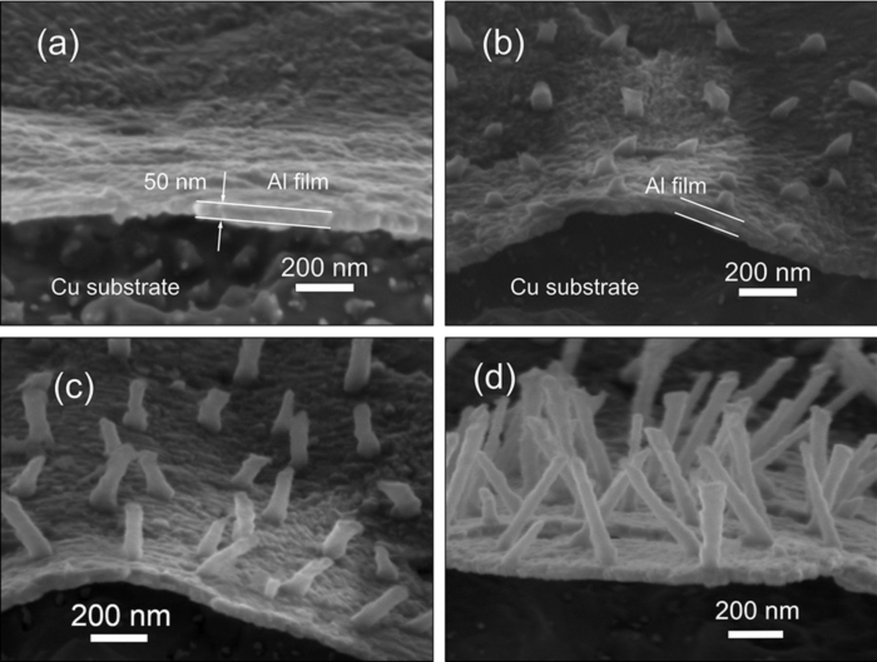
Figure 3. (a) Side view SEM images of the partially peeled-off Al nano thin film acquired in the sample electrodeposited at −1.2 V for 5 s at 25°C on Cu substrate, (b) the Al nano thin film with Al nano-nuclei, (c, d) the Al nano thin film with Al nanowires.
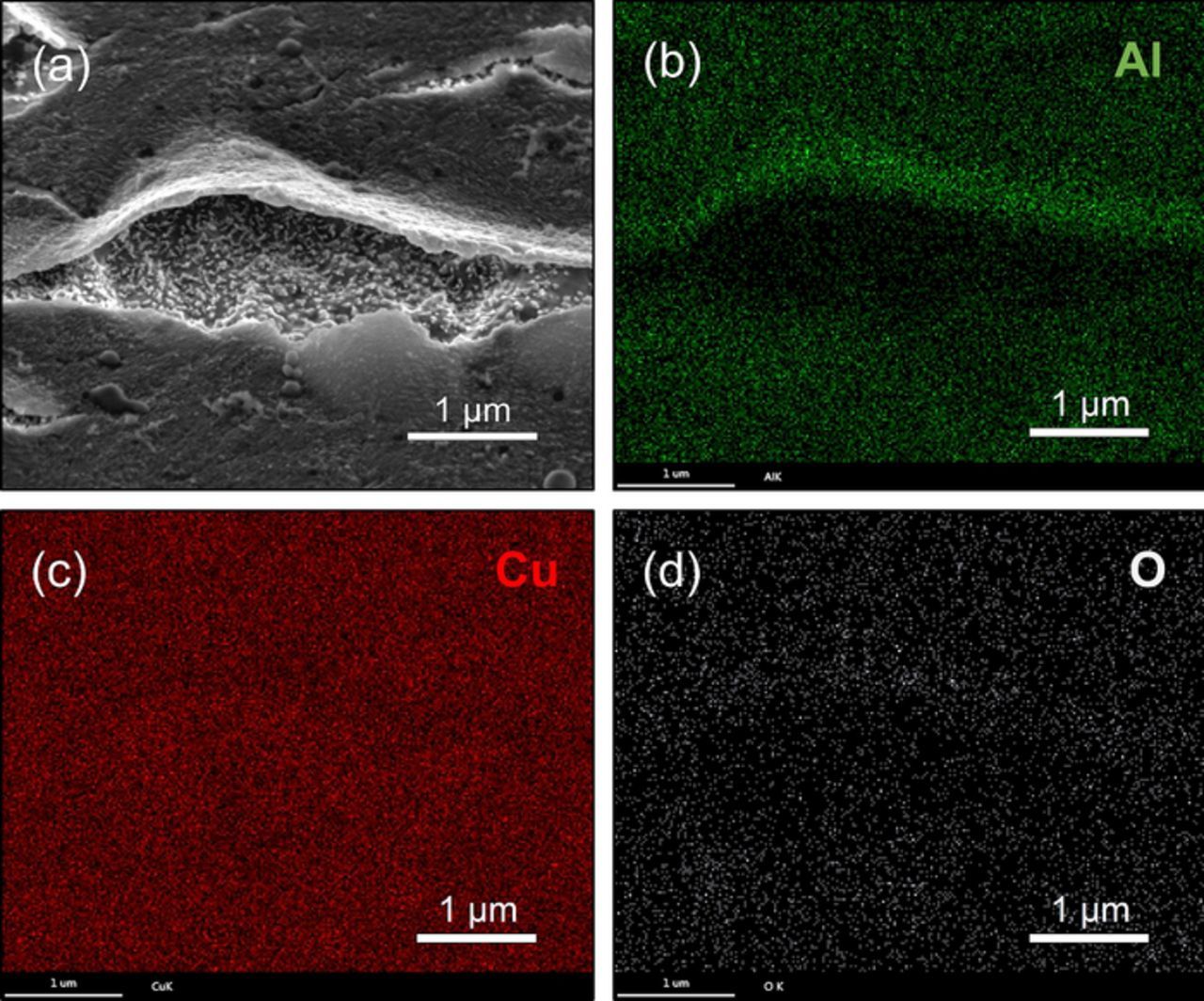
Figure 4. (a) Side view SEM images of the partially peeled-off Al nano thin film acquired in the sample electrodeposited at −1.2 V for 5 s at 25°C on Cu substrate. (b-d) EDS elemental maps of the area shown in (a) showing the distribution of Al, Cu and O.
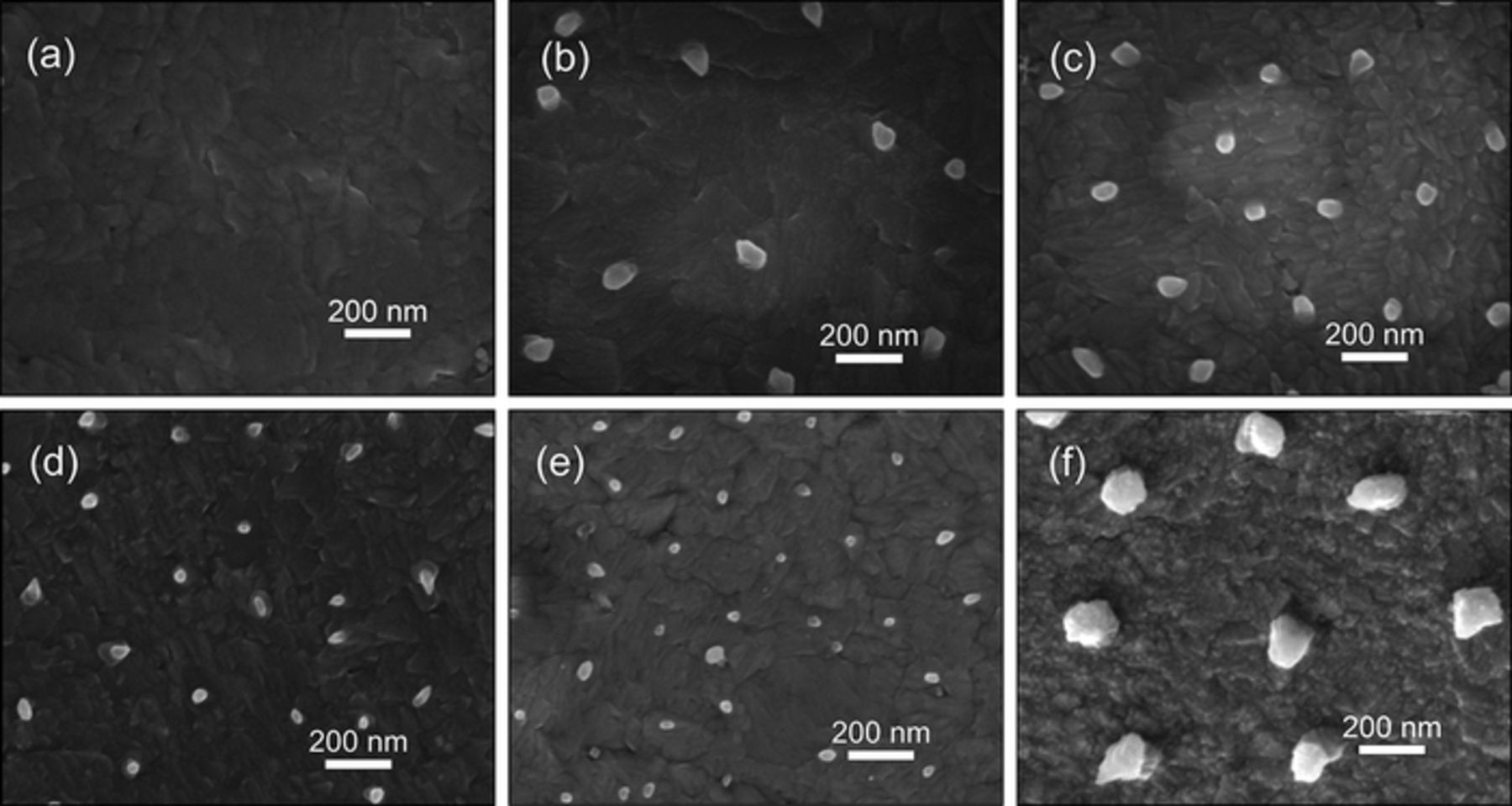
Figure 5. (a) Top view SEM image of the Al nano thin film electrodeposited on Cu substrate at −1.2 V for 5 s at 25°C. Top view SEM images of Al nano-nuclei on the Al nano thin film electrodeposited on Cu substrate for 5 s at −1.0 V/25°C (b), −1.2 V/25°C (c), −1.4 V/25°C (d), −1.6 V/25°C (e) and −1.6 V/50°C (f).
After formation of the Al nano thin film, the nucleation on the Al film firstly occurs on the edge of the Cu electrode located in the middle of the ionic liquid. The nucleation spreads from the edge to the central part of the electrode gradually in several seconds (see Figure S1), indicating the nucleation is controlled by diffusion since the edge part of the Cu electrode acquires more Al2Cl7− from the lateral diffusion. The velocity of the spread of nucleation from the edge to the central part of the electrode increases with the adding of overpotential. Reflected in the chronoamperometry curves (Figure 1b), the length of the current decreasing stage after the current peak decreases with the increase of overpotential. Once the nuclei form, they will grow immediately which means the nano-nuclei shown in Figures 5b–5f are supposed as the initial state of the grown nuclei. Due to the resolution limit, the real size of the Al nuclei cannot be accurately confirmed in our SEM observation. The locations of these nano-nuclei should be related to the defects in the pre-deposited thin film. Those defects provide the active sites where a lower concentration of Al2Cl7− can meet the conditions for nucleation. For example, the active sites for nucleation are considered as the emergence points of the screw dislocations in Reference 42. When the more negative potential is applied, the electrochemical reaction becomes faster and the density of defects in the pre-deposited thin film gets higher. Therefore, the areal density (number of the Al nuclei per unit area) of the Al nano-nuclei also rises from around 5.7 μm−2 at −1.0 V/25°C to 9 μm−2 at −1.2 V/25°C, 12.5 μm−2 at −1.4 V/25°C and 17.7 μm−2 at −1.6 V/25°C. While the areal density sharply declines to about 4.6 μm−2 at −1.6V when the electrodeposition temperature increases to 50°C. The low density of defects in the pre-deposited thin film at 50°C could be ascribed to the rapid atomic migration at the higher reaction temperature. The adsorption of cations of the ionic liquid on the surface of the deposits may also affect the electrodeposition at 50°C since the adsorption is highly dependent on temperature. It is noticeable that the size of the Al nano-nuclei gradually decreases with the increase of overpotential and significantly enlarges at 50°C.
Once arise on the Al nano thin film, the Al nano-nuclei continue growing to Al nanowires. The typical morphologies of the Al nanowires electrodeposited at different potantials are shown in Figures 6a–6d. As exhibited in Figures 6e–6f, the Al nanowires electrodeposited at −1.4 V/25°C can grow to lengths of up to 50 μm in 120 s with an average diameter of about 45 nm, reaching a high aspect ratio over 1000. The average growth rate at −1.4 V/25°C is more than 0.4 μm/s and even higher at −1.6 V or at high temperatures. As we known, it is the fastest process that ever reported on directly electrodeposition for synthesis of 1D structures from ionic liquids. The deposits are of quite uniform morphology over large areas.
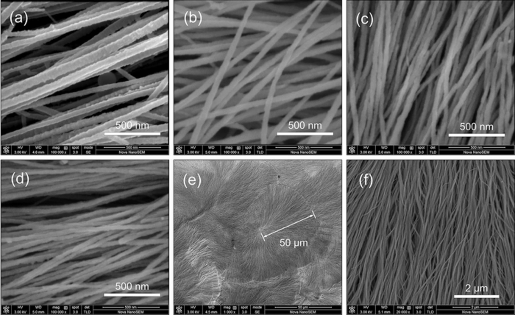
Figure 6. SEM images of Al nanowires electrodeposited at −1.0 V/25°C (a), −1.2 V/25°C (b), −1.4 V/25°C (c) and −1.6 V/25°C (d). (e, f) Low- and High-magnification SEM images of the Al nanowires electrodeposited on Cu substrate at −1.4 V for 120 s at 25°C.
The statistic diameter data as shown in Figure 7 are obtained from analysis of hundreds of Al nanowires in SEM images. In accordance with the size of Al nano-nuclei, the average diameter of Al nanowires also reduces as the overpotential increases however evidently increases at 50°C since both electrochemical reaction and diffusion accelerate at higher temperature. The average diameter of nanowires electrodeposited for 60 s is about 60.4 nm at −1.0 V/25°C, 51.2 nm at −1.2 V/25°C, 42.6 nm at −1.4 V/25°C, 30.7 nm at −1.6 V/25°C and 70.2 nm at −1.6 V/50°C.
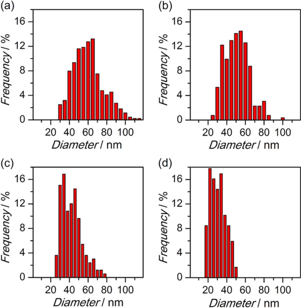
Figure 7. Histograms depicting the diameter distributions of Al nanowire electrodeposited at −1.0 V/25°C (a), −1.2 V/25°C (b), −1.4 V/25°C (c) and −1.6 V/25°C (d).
For the electrodeposition time within 60 s, the average diameter of Al nanowires grow at −1.6 V is approximately constant. The Al2Cl7− depleted zone mentioned above helps the shape maintaining during the growth of Al nanowires. When the Al nanowires grow, Al2Cl7− from bulk ionic liquid quickly diffuse to the tops of the Al nanowires where the reduction of Al2Cl7− mainly occurs. The Al2Cl7− depleted zone next to the pre-deposited Al thin film expands along the direction of the Al nanowires growth and the lateral growth of Al nanowires is restrained since the concentration of Al2Cl7− sharply decreases in the area among the Al nanowires. The obvious lateral growth is found at some tops of Al nanowires electrodeposited at −1.6 V for 120 s that indicate the Al2Cl7− depleted zone can't retain for a long time (Figure 8a). The re-nucleation and following re-growth on the lateral grown tops of Al nanowires are also observed when the deposition time is extended to 150 s (Figure 8b).
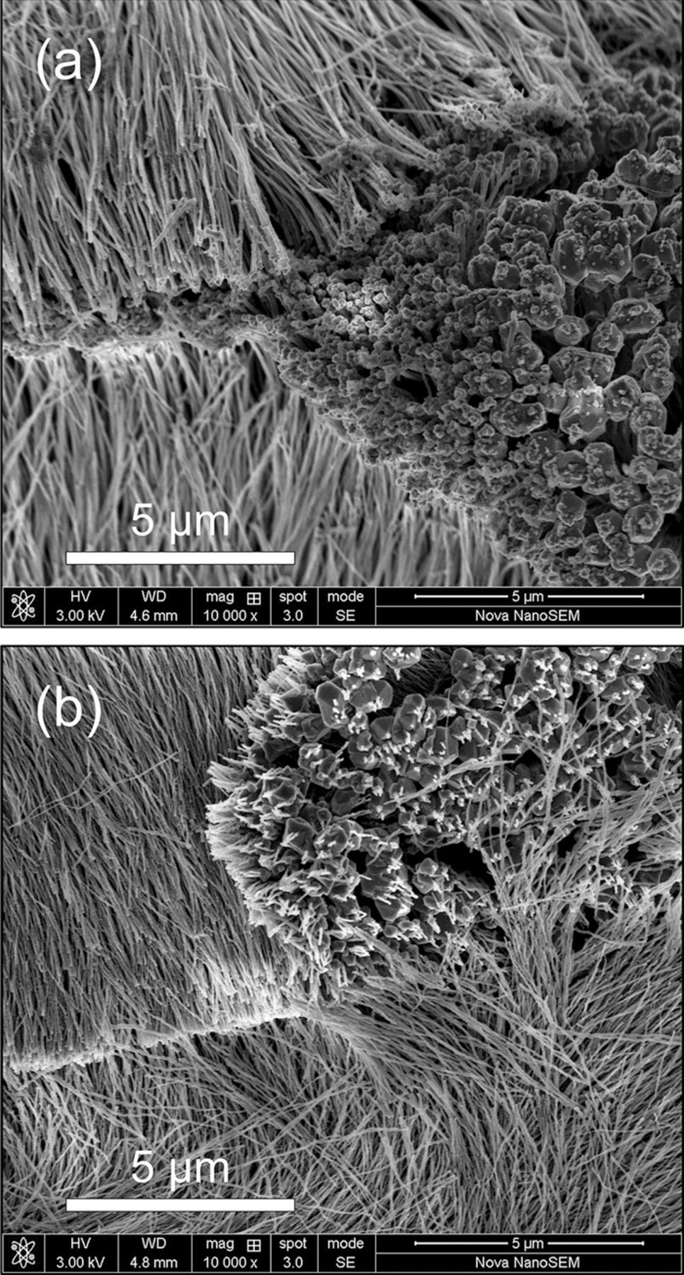
Figure 8. (a) SEM image shows the lateral growth at some tops of Al nanowires electrodeposited at −1.6 V for 120 s at 25°C. (b) SEM image shows the re-nucleation and re-growth on the lateral grown tops of Al nanowires electrodeposited at −1.6 V for 150 s at 25°C.
The number of the Al nanowires per unit area depends on the areal density of the Al nano-nuclei on the pre-deposited Al thin film and also affect the Al2Cl7− depleted zone. Branches are both observed in Al nanowires electrodeposited at −0.8 V/25°C for 120 s and at −1.6 V/50°C for 60 s, implying the secondary growth of Al nanowires in the electrodeposition (Figure 9a). Al nanowires with small branches can be electrodeposited from the AlCl3-BMPC (mole ratio is 1.8:1) ionic liquid at −1.6 V for 60 s at 25°C (Figure 9b). Due to the low areal density of the Al nano-nuclei on the pre-deposited Al thin film, the Al2Cl7− among the Al nanowires can be easily supplemented by diffusion that induce the secondary growth of Al nanowires. Moreover, not all the Al nanowires will grow at the same pace because of the fluctuating concentration of Al2Cl7− around the Al2Cl7− depleted zone. The slight fluctuations in the steady stages of the chronoamperometry curves shown in Figure 1b also reflect the fluctuating of Al2Cl7− concentration during the growth of Al nanowires. Some of the Al nanowires lag behind in the depleted zone and may won't get enough Al2Cl7− to grow again.
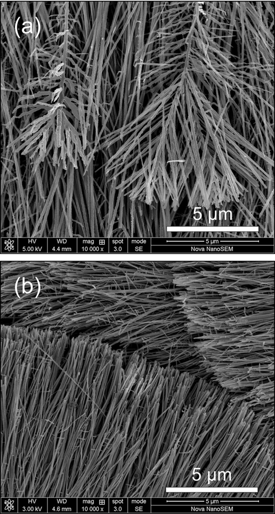
Figure 9. (a) SEM image of the Al nanowires with branches electrodeposited at −1.6 V for 60 s at 50°C from the AlCl3-BMPC (mole ratio is 2:1) ionic liquid. (b) SEM image of the Al nanowires with branches electrodeposited at −1.6 V for 60 s at 25°C from the AlCl3-BMPC (mole ratio is 1.8:1) ionic liquid.
Here we provide another solid evidence for the existence of the Al2Cl7− depleted zone. Once the electrodeposition pauses for a while after formation of the Al nano-nuclei on the pre-deposited Al nano thin film, those Al nano-nuclei grow into submicron sized octahedrons instead of continuing the follow-up 1D growth when the potential is re-applied (see Figure S3). Then the re-nucleation and the following 1D growth of Al nanowires occur both on and around the octahedrons. That imply the Al2Cl7− depleted zone fades away since the diffusion of Al2Cl7− during the experiment pause and the 2D-3D-1D growth process starts over again when the electrodeposition resumes.
As shown in the XRD results, the probability of [200] directional growth raises with the increase of overpotential (see Figure S4). Determined in selected area diffraction patterns and high-resolution TEM images, most of the electrodeposited Al nanowires are single crystalline structures and grow in the [200] direction indicating the {200}/{100} planes grow most quickly (see Figure 10, Figure S5 and Figure S6). As presented in Figure S6, the [200] direction doesn't change during the growth of Al nanowires. The surfaces of some Al nanowires are a bit rough and the 2–5 nm thick oxide layers are also observed in TEM images.
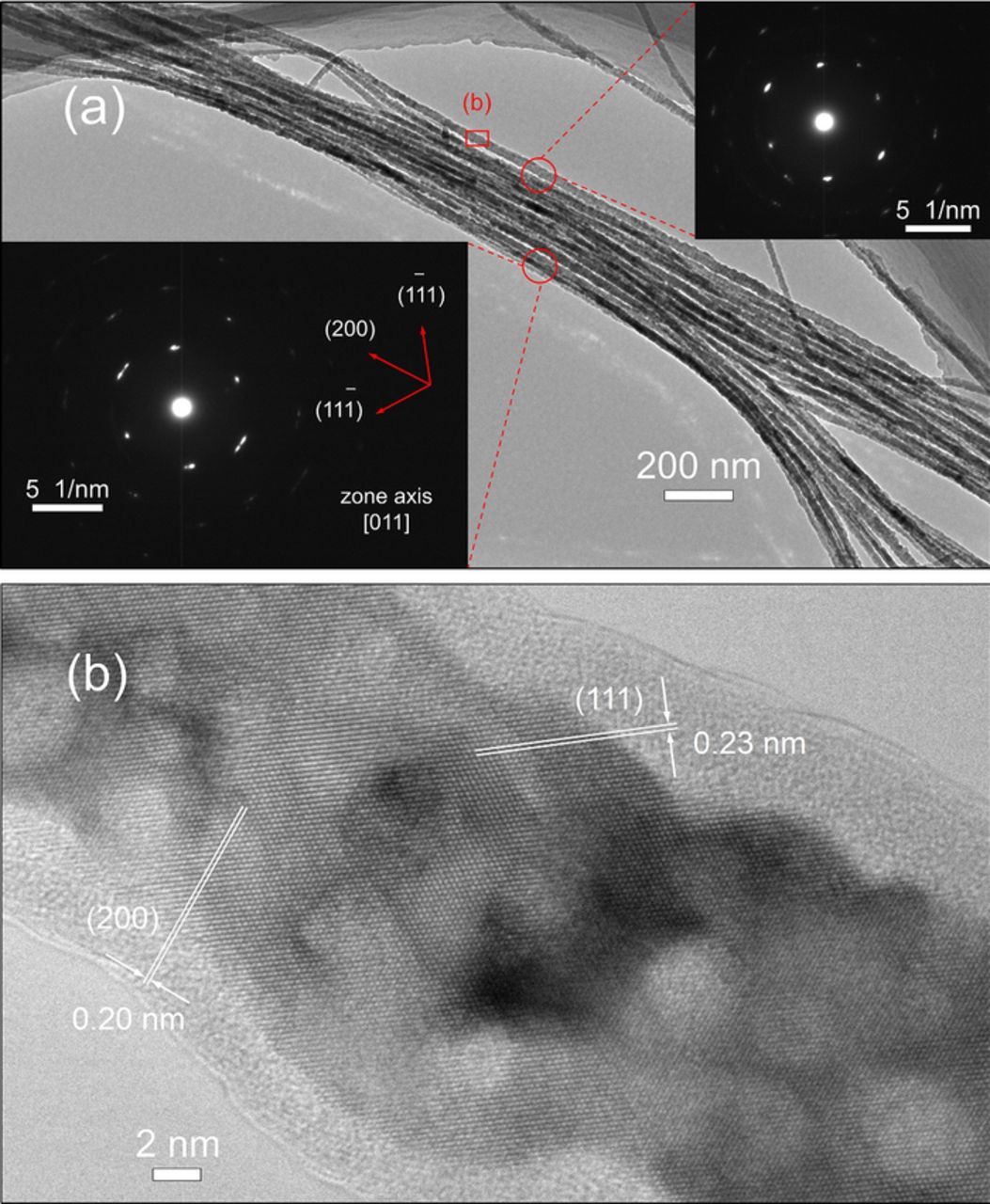
Figure 10. (a) TEM image of Al nanowires electrodeposited at −1.6 V/25°C and two selected area electron diffraction (SAED) patterns from the indicated regions. (b) High-resolution TEM image of the region marked in (a).
Why could these happen in the AlCl3-BMPC ionic liquid? Firstly, the AlCl3-BMPC ionic liquid has a wider electrochemical window than many other chloroaluminate ionic liquids, therefore high overpotential can be realized during electrodeposition. Obvious decomposition of the positive ions ([BMP]+) is not observed in our experiments even when a −1.6 V (vs. Al/Al3+) potential is applied. Then the pyrrolidinium cations play a key role in the formation of Al nanocrystalline thin film which is demonstrated in Reference 43. It is found that the pyrrolidinium cations interfere with the substrate differently than the common used imidazolium cations.44 Moreover, the diffusion of Al2Cl7− in AlCl3-BMPC (2:1 mole ratio) is compatible with the electrochemical reaction on the top of Al nanowires that the Al2Cl7− depleted zone can be maintained and further expand with the growth of Al nanowires. In our measurement, the viscosity of AlCl3-BMPC (2:1 mole ratio) is 39.7 mPa·s at 25°C, which is much higher than the viscosity of the common used AlCl3-EMIC (2:1 mole ratio) ionic liquid (about 14 mPa·s at 25°C according to Reference 45). The relatively high viscosity of the ionic liquid reduces the diffusion rate of Al2Cl7− and make it easier to form and extend the Al2Cl7− depleted zone than the low viscosity electrolytes.36 Hence the Al nano-nuclei could evenly form on the pre-deposited Al thin film and 1D growth of Al nanowires could continue for a period of time.
Conclusions
Single-crystalline Al nanowires with high aspect ratios can be directly electrodeposited from the AlCl3-BMPC room temperature ionic liquid without using templates, additives or catalysts. The electrochemical 2D nanofilm-3D nanonuclei-1D nanowires (EC 2D-3D-1D) growth mechanism is proposed for the first time. We demonstrate the nanowire dimensions are well controlled through the variation of electrode potential, temperature and growth time. The diffusion has great influence on the growth process. This one-step, ultra-fast and performable at room temperature approach should be substantial for low-cost mass-producing high-quality nanowires and may have applications in fabrication of nanowire-based devices.
Acknowledgments
This work was financially supported by National Natural Science Foundation of China (No. 51474107). The authors thank Nan Song for assistance during SEM observation.
ORCID
Bing Li 0000-0002-1082-5853